Every iPhone chip, AI processor, and data center GPU ultimately traces its roots back to a place cleaner than any hospital on Earth — a semiconductor cleanroom.
And when it comes to the cleanest and most advanced, TSMC’s 3nm and 2nm fabs in Taiwan lead the world. These facilities don’t just build chips; they define the limits of computing itself.
The World’s Most Advanced Factories
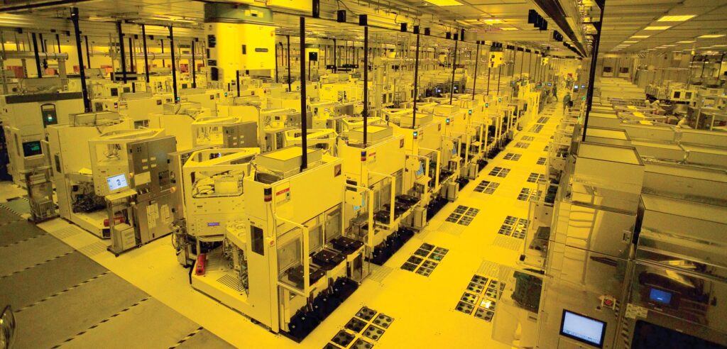
TSMC’s Fab 18 in Tainan is the beating heart of 3nm production — a “giga-fab” composed of multiple interconnected phases. Each phase has around 58,000 square meters of cleanroom space, with the total footprint spanning well over 160,000 square meters.
The scale is staggering — imagine dozens of football fields filled with robotic arms, vacuum chambers, and EUV scanners worth hundreds of millions each. And every square inch must remain free of dust, vibration, or temperature drift that could destroy chips measured in atoms.
Cleanroom Precision: Where Physics Meets Perfection
1. Particle Control
At 3nm and 2nm scales, even a single microscopic particle can ruin an entire wafer.
TSMC maintains ISO Class 3–5 cleanrooms, meaning there are fewer than 1,000 particles per cubic meter — that’s about 10,000× cleaner than a hospital operating room.
Air flows in laminar patterns, replacing the entire room’s atmosphere hundreds of times per hour to keep it pristine.
2. Temperature and Humidity Stability
EUV lithography — which prints chip features using 13.5 nm light — requires temperature control as tight as ±0.01°C.
A change of just one-hundredth of a degree can cause nanometer-scale misalignments in the wafer patterning, breaking billions of transistors.
3. Vibration Isolation
The floors of these fabs are mounted on active vibration-damping systems, ensuring even passing trucks or small earthquakes don’t affect the ultra-fine laser alignments of lithography tools.
4. Chemical and Air Filtration
Advanced filters remove molecular contaminants — acids, bases, and organics — that could degrade EUV mirrors or photoresists. The air is continuously purified through multi-stage filtration to maintain chemical stability.
The Magic of EUV: Light Smaller Than Light
TSMC’s 3nm node uses ASML’s EUV (Extreme Ultraviolet) lithography machines, each costing around $200 million. These systems use powerful CO₂ lasers that vaporize tiny tin droplets, creating plasma hotter than the surface of the sun — all to emit light at a wavelength of just 13.5 nm.
That light bounces through an intricate set of mirrors (no lenses — glass would absorb EUV) before etching transistor patterns onto silicon wafers.
At 2nm, TSMC will transition to High-NA EUV, a next-generation system with even higher resolution.
What Changes at 2nm: The GAA Revolution
While 3nm relies on FinFET transistors, the upcoming 2nm (N2) node introduces Gate-All-Around (GAA) nanosheets, allowing even greater control of current flow through the transistor.
TSMC is also adding backside power delivery, called the Super Power Rail (SPR).
By routing power beneath the transistor instead of above it, TSMC reduces resistance, improves efficiency, and frees up valuable space for more logic — meaning higher performance and lower energy use.
Why Cleanrooms Define Computing Power
A cleanroom isn’t just a sterile workspace — it’s a precision ecosystem.
Every variable — air pressure, temperature, humidity, vibration — directly affects transistor alignment, yield, and performance.
At these scales, controlling the environment is as important as the chip design itself. A single unnoticed particle or temperature drift could turn a billion-dollar production run into waste.
The Cost of Perfection
Each phase of TSMC’s Fab 18 costs billions to construct.
Every EUV scanner consumes enough electricity to power hundreds of homes, and the facility’s energy, gas, and chemical systems operate 24/7.
But this investment pays off — 3nm chips now power iPhones, MacBooks, and AI processors, while 2nm will anchor the next generation of supercomputers, smartphones, and autonomous systems.
What It Means for the Future
As AI models grow, and data centers demand faster, denser, and more efficient chips, cleanrooms like those at TSMC become the hidden foundation of the digital world.
Without them, there would be no ChatGPT, no quantum simulation chips, no AI-driven cars — because none of these technologies can exist without the atomic precision forged in these silent, sterile halls.