Every time you tap on your smartphone, train an AI model, or launch a rocket — you’re relying on patterns etched by light.
That light comes from a technology so advanced, only one company on Earth can make it work: ASML.
Welcome to EUV lithography — the technology that made 3 nm and 2 nm chips possible, and the reason ASML became one of the most strategically important companies in the world.
What Is Lithography?
In simple terms, lithography is the process of printing circuits onto silicon wafers.
Think of it as the world’s most precise projector: it shines light through a stencil (called a mask) to draw microscopic transistor patterns.
But as chips got smaller — from 90 nm to 7 nm and now 3 nm — ordinary light wasn’t sharp enough.
To keep shrinking transistors, the industry needed a new kind of light.
Enter EUV: Extreme Ultraviolet Light
EUV stands for Extreme Ultraviolet, with a wavelength of 13.5 nanometers — about 15 times smaller than deep ultraviolet (DUV) light used before.
That tiny wavelength lets engineers draw features just a few atoms wide — enabling modern processors like Apple’s M3, NVIDIA’s H200, and AMD’s Zen 5.
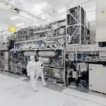
But generating EUV isn’t just difficult — it’s one of the hardest engineering challenges ever solved.
How It Works (In Mind-Blowing Detail)
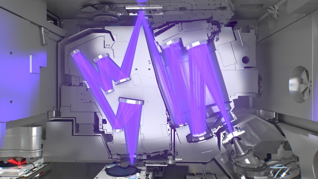
- A tin droplet (about the size of a red blood cell) is fired through a vacuum.
- A powerful CO₂ laser hits it twice — first to flatten it, then to vaporize it.
- The explosion creates a plasma hotter than the sun’s surface, emitting EUV light.
- That light bounces off a series of ultra-precise mirrors before hitting the wafer.
No lenses. No air. No room for error.
Even a single speck of dust could ruin the entire beam.
Why Only ASML Can Do It
Because no one else can.
- Complexity: Each EUV machine contains over 100,000 parts and over 2 kilometers of cabling.
- Cost: A single EUV system costs around $200 million — and weighs 180 tons.
- Collaboration: ASML integrates technologies from hundreds of suppliers —
- Carl Zeiss (Germany) makes the ultra-precise mirrors.
- Trumpf (Germany) builds the CO₂ lasers.
- Cymer (U.S.) provides the plasma light source.
No other company has managed to combine all these systems with the required precision.
The Monopoly No One Can Break
ASML spent over 20 years and billions of dollars developing EUV before selling a single machine.
Intel, TSMC, and Samsung all funded parts of that research — because without EUV, their roadmaps would have ended at 7 nm.
Now, every advanced chip on Earth — from Apple’s A17 Pro to NVIDIA’s Blackwell GB200 — is made using ASML machines.
That gives ASML a de facto monopoly on the future of computing.
Beyond EUV: The Next Leap
ASML is already working on High-NA EUV, which uses larger numerical apertures for even finer patterning — down to 1.4 nm class features.
These machines will cost over $350 million each, and TSMC, Intel, and Samsung have all placed their first orders.
It’s not just chipmaking anymore — it’s a race for atomic-scale manufacturing.
Why EUV Matters
EUV lithography is the invisible backbone of progress in:
- AI chips (NVIDIA, AMD, Google TPU)
- Smartphones (Apple, Qualcomm, MediaTek)
- Data centers, cars, and quantum hardware
Every layer of technological civilization — from cloud servers to self-driving cars — runs on patterns carved by ASML’s light.
The Bigger Picture
ASML isn’t just a company; it’s a geopolitical asset.
Its technology sits at the center of U.S.–China trade tensions, global supply chain strategies, and even military policy.
Whoever controls access to EUV controls access to the future of semiconductors.
And right now — that future runs through a small town in Veldhoven, Netherlands.