The future of artificial intelligence just got dramatically more energy-efficient. Researchers at the University of Florida have developed a groundbreaking silicon photonic chip that uses light instead of electricity to perform AI computations, achieving up to 100-fold improvements in power efficiency while maintaining near-perfect accuracy.
The Energy Crisis in AI Computing
Artificial intelligence is experiencing unprecedented growth, but this expansion comes with a significant environmental cost. Current AI systems consume enormous amounts of electricity for training and inference tasks, with data centers housing AI workloads accounting for an increasingly large portion of global energy consumption.
The most power-intensive aspect of AI computing involves convolution operations—the mathematical backbone of image recognition, pattern detection, and many other AI tasks. Traditional silicon chips perform these calculations using electrons, which generates heat and requires substantial energy input.
How Light-Based Computing Changes Everything
The University of Florida research team, led by experts from the Florida Semiconductor Institute, has fundamentally reimagined how AI computations can be performed. By etching microscopic lenses directly onto silicon, they’ve enabled laser-powered computations that cut power use dramatically while maintaining near-perfect accuracy.
The Science Behind Photonic AI Processing
The breakthrough centers on using light photons rather than electrons to perform mathematical operations. Here’s how the revolutionary process works:
Data Encoding: Information is encoded into laser light directly on the chip, converting digital data into optical signals that can be manipulated using photonic components.
Fresnel Lens Processing: The prototype chip uses two sets of miniature Fresnel lenses using standard manufacturing processes. These two-dimensional versions of the same lenses found in lighthouses are just a fraction of the width of a human hair.
Optical Convolution: The Fresnel lenses act as spatial filters that perform the multiply-and-add operations essential to AI tasks. As light passes through these lenses, the mathematical operations occur naturally through the physical properties of light interaction.
Digital Conversion: The processed optical signals are converted back to digital format, completing the computational cycle with dramatically reduced energy consumption.
Unprecedented Performance Results
The research team’s prototype has demonstrated remarkable capabilities in real-world testing scenarios:
Accuracy Benchmarks
In tests, the new chip successfully classified handwritten digits with about 98% accuracy, on par with traditional chips. This performance level proves that optical computing can match conventional silicon-based AI processors without sacrificing precision.
Power Efficiency Gains
The most striking achievement is the dramatic reduction in energy consumption. The optical approach delivers 10x to 100x less power usage for identical AI tasks, representing a quantum leap in computational efficiency.
Speed Advantages
Beyond power savings, the light-based system also provides significant speed improvements. Since photonic operations occur at the speed of light and multiple wavelengths can be processed simultaneously, the chip can handle more data in parallel than traditional electronic systems.
Technical Innovation: Wavelength Division Multiplexing
One of the most ingenious aspects of this breakthrough is the implementation of wavelength division multiplexing. Since different colors of light don’t interfere with each other, multiple data streams can be processed simultaneously through the same set of Fresnel lenses.
This parallel processing capability means that a single optical chip can handle multiple AI tasks concurrently, dramatically increasing throughput without proportional increases in power consumption or physical chip size.
Manufacturing Advantages and Scalability
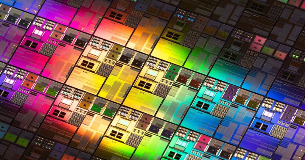
The University of Florida team designed their optical chip using standard semiconductor manufacturing processes, making it compatible with existing chip fabrication infrastructure. Each lens is narrower than a human hair and etched onto the chip with standard semiconductor techniques.
This compatibility is crucial for commercial viability, as it means the optical chips can be produced using existing manufacturing facilities without requiring entirely new production lines or specialized equipment.
Real-World Applications and Impact
Data Centers and Cloud Computing
The immediate beneficiaries of this technology will be data centers running AI workloads. A 100-fold reduction in power consumption could dramatically reduce the operational costs of AI services while making them more environmentally sustainable.
Edge AI Devices
The power efficiency improvements make it feasible to run sophisticated AI tasks on battery-powered edge devices, from smartphones to autonomous vehicles, without rapidly draining power sources.
Scientific Research and High-Performance Computing
Research institutions conducting AI-intensive work, such as climate modeling, drug discovery, and astronomical data analysis, could achieve the same results with significantly lower energy budgets.
Consumer Electronics
The integration of efficient AI processing could enable more sophisticated features in consumer devices while extending battery life—a crucial factor in portable technology adoption.
Collaborative Research Excellence
This breakthrough represents a collaborative effort involving multiple prestigious institutions. The research team includes experts from the University of Florida, UCLA, and George Washington University, demonstrating the power of cross-institutional collaboration in tackling complex technological challenges.
The work emerged from the Florida Semiconductor Institute, positioning Florida as a leader in next-generation computing technologies and potentially attracting further investment in optical computing research and development.
Current Limitations and Future Development
While the results are promising, the researchers have identified two key challenges that must be addressed for widespread commercial adoption:
Data Transfer Optimization
Moving data efficiently across the optical-electronic boundary remains a technical hurdle. The conversion between optical and electronic signals must be optimized to maintain the overall efficiency gains achieved by optical processing.
Laser Power Management
Managing laser power consumption and minimizing optical losses throughout the system are critical for maintaining the energy efficiency advantages. The team is working on optimizing laser efficiency and reducing power requirements for the optical components.
The Path to Commercial Implementation
The research team envisions a hybrid approach where optical convolution blocks work alongside traditional digital processing cores. This integration strategy would allow manufacturers to incorporate the power-saving benefits of optical computing while maintaining compatibility with existing software and hardware ecosystems.
The modular approach means that optical processing units could be added to current chip designs to handle the most power-intensive AI tasks, while conventional electronics continue to manage other computational requirements.
Industry Implications and Market Potential
Competitive Advantages
Companies that successfully integrate optical AI processing could gain significant competitive advantages through:
- Reduced operational costs in data centers
- Enhanced battery life in mobile applications
- Improved performance in real-time AI applications
- Lower environmental impact and improved sustainability metrics
Investment Opportunities
The breakthrough opens new investment opportunities in:
- Optical computing component manufacturing
- Hybrid chip design and production
- Specialized software optimized for optical processing
- Infrastructure upgrades for optical-enhanced data centers
Environmental and Economic Benefits
The environmental implications of this technology are substantial. If widely adopted, optical AI chips could significantly reduce the carbon footprint of the global AI industry. With AI computing demand projected to continue growing exponentially, efficiency improvements of this magnitude could prevent massive increases in energy consumption.
From an economic perspective, the reduced power requirements could make AI capabilities more accessible to organizations with limited energy budgets, democratizing access to advanced AI technologies globally.
Future Research Directions
The success of this initial prototype opens several avenues for future research and development:
Advanced Optical Architectures
Researchers are exploring more complex optical processing architectures that could handle a broader range of AI tasks beyond convolution operations.
Integration with Quantum Computing
The intersection of optical computing and quantum processing could yield even more dramatic performance improvements for specific AI applications.
Specialized Applications
Custom optical processors designed for specific AI tasks, such as natural language processing or computer vision, could achieve even greater efficiency gains.
Manufacturing Scale-Up
Research into mass production techniques for optical AI chips will be crucial for bringing costs down to commercially viable levels.
Timeline for Commercial Deployment
While still in the research phase, the use of standard semiconductor manufacturing processes suggests that commercial applications could emerge within the next 5-10 years. Early adoption will likely occur in high-performance computing applications where the power savings justify any additional costs, followed by broader consumer applications as manufacturing scales up and costs decrease.
Conclusion: A New Era of Efficient AI Computing
The University of Florida’s breakthrough in optical AI processing represents a fundamental shift in how we approach artificial intelligence computation. By harnessing the natural properties of light to perform mathematical operations, researchers have demonstrated that dramatic improvements in energy efficiency are not only possible but achievable with existing manufacturing technologies.
As the AI industry grapples with growing energy demands and environmental concerns, innovations like optical computing offer a path toward sustainable growth. The combination of improved performance, reduced power consumption, and manufacturing compatibility positions this technology as a potential game-changer for the entire AI ecosystem.
The next phase of development will focus on overcoming the remaining technical challenges and preparing for commercial implementation. If successful, light-based AI chips could reshape not just how we compute, but how we think about the relationship between technological advancement and environmental responsibility.
This breakthrough demonstrates that the future of AI doesn’t just lie in more powerful processors, but in fundamentally more efficient approaches to computation. As researchers continue to refine this technology, we may be witnessing the dawn of a new era where AI capabilities can grow without proportional increases in energy consumption—a crucial development for the sustainable future of artificial intelligence.

